#Amplifier,#Limiter,#Bias tees,........
RF/Microwave Products Customizations
LogicMW – Professional Supplier of RF and Millimeter Wave Solutions (DC-40GHz)
LogicMW – Professional Supplier of RF and Millimeter Wave Solutions (DC-40GHz)
Product classification

Amplifier
LNA Series (Low Noise Amplifier Modules): Ideal for weak sig···

Filter
FLT Series (Bandpass Filters): Filters unwanted frequencies,···

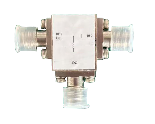
Bias-Tee
BT Series (Bias Tees): Combines DC power and RF signals, sui···

Attenuator
ATT Series (RF Attenuators): Adjusts signal amplitude precis···

Power Divider
PD Series (Power Dividers): Splits RF power into m···

Mixer
MIX Series (RF Mixers): Converts signal frequencie···

Limiter
LIM Series (RF Limiters): Protects sensitive compo···

Front-End Modules
FE Series (Integrated Front-End Modules): Combines···
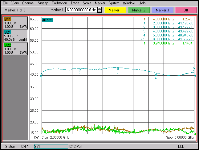
9-9.6GHz
Band Pass Filter
Bandpass filter is a filter used to solve the radiation interference.
• Frequency Range: 9-9.6GHz
• Insertion:0.7dB

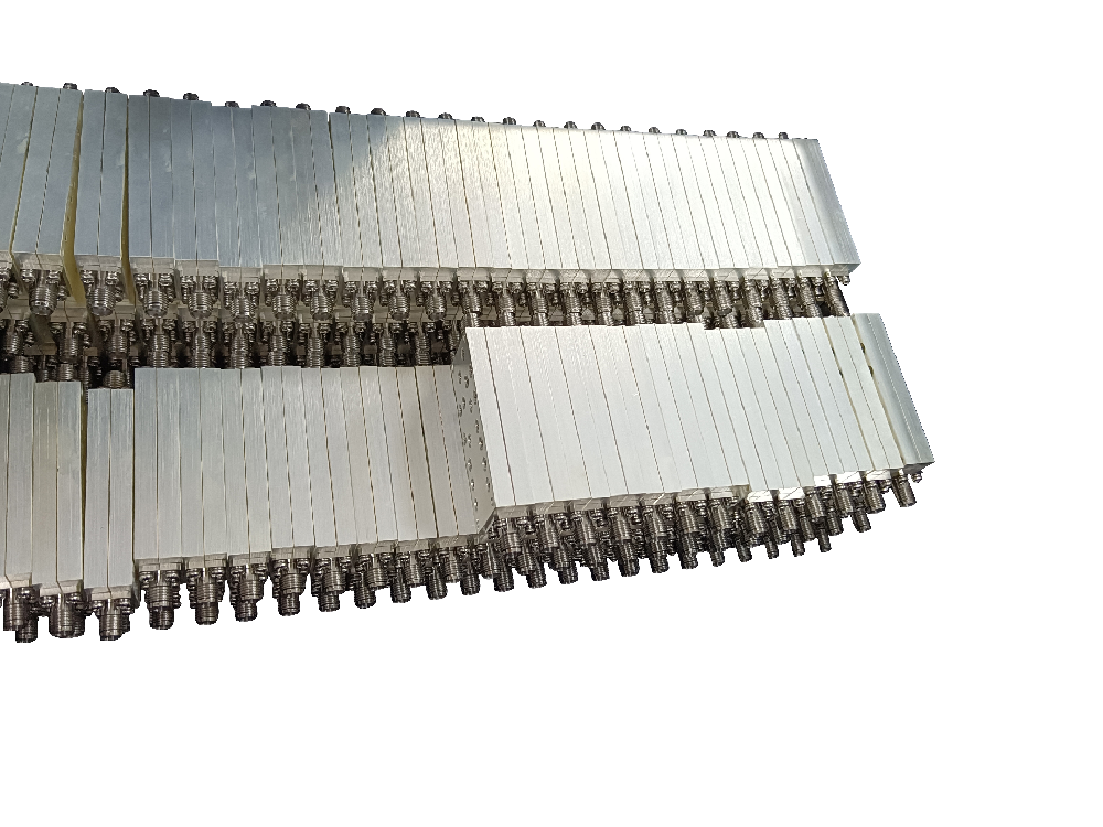
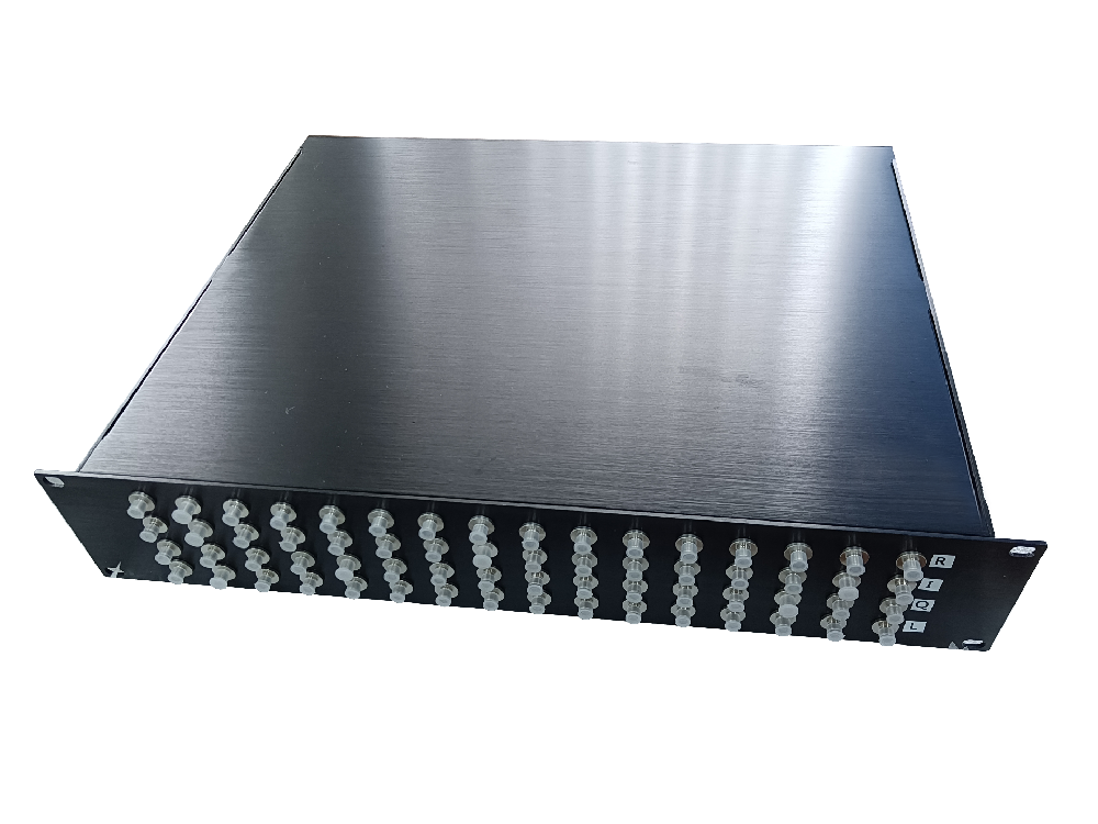
#64-channel
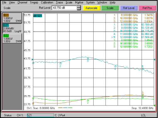
IQ modulator system integrated chassis
• Wideband RF & LO, 4GHz to 8.5GHz
• Wideband IF, DC to 3500 MHz
• Image Rejection, Typ. 25 dBc
• High LO-RF Isolation, Typ. 42 dB
• High Input IP3, Typ. +20 dBm
• Usable as Image Reject Mixer & SSB Converter
APPLICATIONS
• Test and Measurement Equipment
• Back Haul Radio
• Satellite Communications
• Radar, EW, and ECM Defense Systems
Note: If this product does not meet your requirements, you can contact us for consultation and to customize the corresponding RF and microwave devices.
Resources
- RF/Microwave Bias Tees from Theory to Practice RF/Microwave Bias Tees··· Top 2024-08-06
- What is a PLL Synthesizer? What is a PLL Synthesi··· 2025-12-13
- Understanding the Operation of the Frequency Synth··· Understanding the Oper··· 2025-12-13
- How to successfully apply a DC bias onto an RF lin··· How to successfully ap··· 2025-12-11
- Why are bias tees necessary for broadband microwav··· Why are bias tees nece··· 2025-12-11
- 5 Ways to Compensate for Passive IQ Mixer Imbalanc··· 5 Ways to Compensate f··· 2025-12-20
- 5 Ways to Compensate for Passive IQ Mixer Imbalanc··· 5 Ways to Compensate f··· 2025-12-20
- 4 Ways to Implement a High Isolation Duplexer for ··· 4 Ways to Implement a ··· 2025-12-20
- Overcoming RF Design Challenges: Strategies and So··· Overcoming RF Design C··· 2025-12-11
- VSWR and Return Loss Calculations VSWR and Return Loss C··· 2025-12-01
Partners