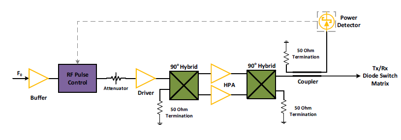
RF POWER AMPLIFIER BLOCK DIAGRAM
The simplified workflow of the RF Power Amplifier is as follows:
The input RF Pulse signal first enters the system and passes through a Buffer stage for initial signal conditioning and isolation.
The conditioned signal is then amplified by a Driver to boost its strength to a level suitable for subsequent stages.
An Attenuator adjusts the signal amplitude precisely to meet the input requirements of the High Power Amplifier (HPA).
The HPA, the core amplification component, further amplifies the signal to the desired high power level.
A Coupler taps off a portion of the amplified signal for monitoring or feedback purposes.
The main signal is routed through two cascaded 90° Hybrids, which manage signal phase and power distribution.
A Diode Switch (Tx/Rx) controls the signal path, enabling switching between transmission (Tx) and reception (Rx) modes as needed.
The Control Matrix oversees the overall operation of the system, coordinating the functions of the switch and other components.
Detector circuits monitor signal parameters (e.g., power level) for feedback and system regulation.
50 Ohm Terminations are integrated at key points to ensure impedance matching, preventing signal reflection and optimizing system performance. The final processed RF signal is then output for transmission.
Previous:Ka BAND VSAT BLOCK DIAGRAM
Next:{contePreviousnextcontent}

