Applications
LogicMW – Professional Supplier of RF and Millimeter Wave Solutions
Position:Index>Applications
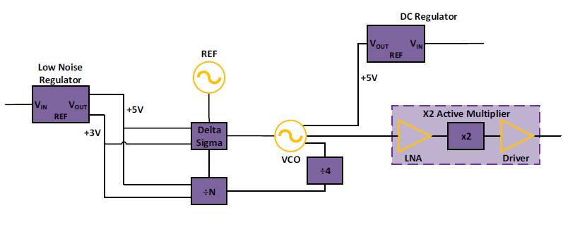
Ka BAND PHASE LOCKED OSCILLATOR BLOCK DIAGRAM
2025-12-23

Ka BAND PHASE LOCKED OSCILLATOR BLOCK DIAGRAM
This Block diagram illustrates a frequency synthesis & signal conditioning system (typically for RF applications), with key functions and components:
Purpose: Generates a high-precision, high-frequency RF signal (via synthesis and multiplication) while maintaining stable, low-noise power supplies—critical for applications like communication transceivers or test equipment.
Previous:I/Q RECEIVER/DOWNCONVERTER BLOCK DIAGRAM
Next:{contePreviousnextcontent}
 )
)
 , generating a precise output frequency.
 for feedback, while the main VCO signal feeds the next stage.
 doubles the frequency.